
Published on the 11th December 2018 by ANSTO Staff
A large international collaboration including scientists from Monash University, the ARC Centre for Future Low Energy Electronics (FLEET), the Monash Centre for Anatomically Thin Materials and the Australian Synchrotron reported today in Nature on progress towards the development of a new generation of ultra-low energy electronics at room temperature.
The research was focused on the development of an advanced material that is able to switch between an electrically conductive state to an insulating state, simply by applying an electric field.

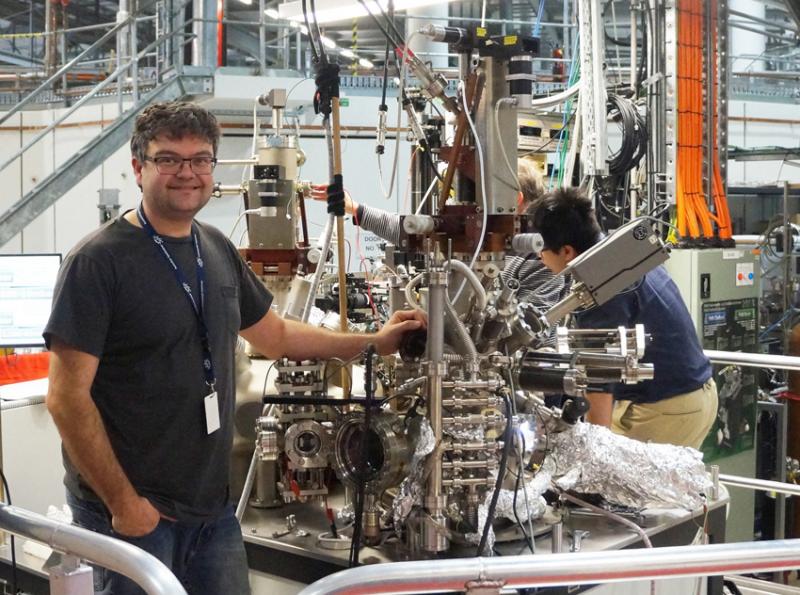
Co-author Dr Anton Tadich, a beamline scientist at the Soft X-ray beamline and Partner Investigator with FLEET, collaborated with investigators from Monash University, Singapore and Lawrence Berkeley National Lab on the use of photoemission techniques at the Australian Synchrotron X-ray Photoelectron Spectroscopy (XPS) and the Advanced Light Source in the US Angle Resolved Photoelectron Spectroscopy, (ARPES).
The chemical composition and growth mechanisms of thin films of the topological Dirac semi-metal sodium bismuthide Na3Bi on a silicon substrate was investigated using XPS at the Australian Synchrotron’s Soft X-ray beamline.
“The variable energy of synchrotron x-rays was able to highlight the chemistry of the topmost layers of the surface with high precision. The measurements provided a unique complement to the scanning tunnelling microscopy (STM) performed at Monash and ARPES experiments performed at Berkley,” said Tadich.
Although STM is very useful for local structural and electronic studies at the surface, it does not provide information about the chemical composition of the film nor the properties of its interface with the silicon substrate.
“Soft x-ray XPS at the Australian Synchrotron confirmed that the material was chemically pure, and, furthermore, did not chemically interact in any way with the silicon underneath, “said Tadich.
“This was important as any bonding with the substrate could possibly affect the tuneable electronic properties of the topological material,” said Tadich.
“It was the ideal phase for experiments involving the application of an electric field to switch it from topological insulator to conventional insulator.”
In order to apply an electric field, the investigators doped the material with sodium, and also probed it with scanning tunnelling microscopy. In both cases, the band gap of the material was able to be closed and reopened, reflecting a quantum phase transition between a so called topological insulator (electrically conductive on the edges of the film), to conventional insulator.
Being able to use an electric field to switch a material back and forth from a conventional insulator to a topological insulator provides the groundwork required to design a “topological transistor”.
In these devices when the transistor is “on”, the electric current only flows along the edges of the material. These special edge-path currents are subject to far less back-scattering (conventional) electrical resistance than in the materials used in conventional transistors—requiring less power consumption.
Unlike superconducting materials which require extremely low temperatures, topological insulators can perform at room temperature.
Topological materials are a major research focus at FLEET.
Other collaborators included researchers from Singapore University of Technology, National University of Singapore, and Yale-NUS College in Singapore
DOI: 10.1038/s41586-018-0788-5
Read the article from FLEET
Read the media release


