
Published on the 9th February 2024 by ANSTO Staff
Key Points
-
ETH Zurich is exploring collaborations with the Centre for Accelerator Science
-
A team led by Prof Dr Ulrike Grossner were at ANSTO to investigate the radiation effects on silicon carbide semiconductors for power applications
-
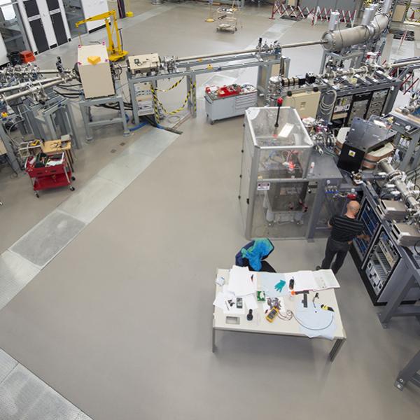
Experiments were conducted using ion microbeam irradiation on the Sirius accelerator at the Centre
A research team from ETH Zurich developing and characterizing silicon carbide devices for power electronics, recently spent time at ANSTO’s Centre for Accelerator Science to use a specialised beamline in their investigations.
Professor Ulrike Grossner, leader of the Advanced Power Semiconductor Laboratory at ETH Zurich, said the precise beam positioning and suite of ions available on the Sirius accelerator were perfect for the type of investigation her team was exploring.
Based in Switzerland, Prof Grossner’s team travelled to the Centre for Accelerator Science because there are very few facilities in the world where this research can be undertaken, where the ANSTO facility stands out for its high flexibility and precision.
The Sirius accelerator has been optimised for radiation testing of electronic components, power devices and photovoltaic technologies.
The ETH team was assisted by accelerator scientist Dr Stefania Peracchi, who has expertise in accelerator technologies for testing radiation effects for space research, together with Senior Instrument Scientist Dr Zeljko Pastuovic and Mechatronic Engineer Dr Ryan Drury.
The ETH Zurich team evaluates and optimises materials and devices to improve their performance and reliability.
“We have specific expertise in silicon carbide (SiC), a promising new semiconductor material for power electronics,“ said Prof Grossner.
“There is still quite a lot that we don’t know about this material.”
“We had the chance to know about the CAS unique microbeam facility through a presentation given by Stefania at an international conference about radiation effects on electronics. We realised it would have been a great opportunity to use their precision irradiation capabilities, so we submitted a proposal”, said senior scientist Corinna Martinella.
The group used the microbeamline to progress an understanding of the radiation effects on specific areas of components that were irradiated with micrometer-precision using focused protons and heavier ion beams.
“The facility is unique as it provides an opportunity to explore the effects of radiation, enabling design changes resulting in radiation hardening”.
They brought multiple samples and prepared a custom sample environment for the tiny electronics to be irradiated.
“We are very grateful to Stefania for her assistance in providing support planning the experimental campaign and all information about the instrument that enabled our team to construct this sample holder for the instrument chamber before our arrival, “ said Prof Grossner.
The visit was an opportunity for team members to gain hands on experience using ion beam irradiation.
The team included two PhD students, Helton Goncalves de Medeiros and Manuel Belanche Guadas, who worked on the preparation of the samples, the irradiations, and will perform post-irradiation analysis.
“During the visit we also explored a possible collaboration between ANSTO and ETH Zurich which will allow investigation of further questions in the field of radiation hardness of SiC devices in harsh environments such as space and high energy physics”, said Dr Peracchi.
Prof Grossner said she was very pleased with experiments and is already thinking about other ideas to test using the accelerators.
She expects the team to have forthcoming journal publications relating to the research.


